Latest from Semivision Substack
From Wafer to System: AIM Photonics and the Rise of America’s Full-Stack PIC FoundryOriginal Articles By SemiVision Research (IEEE ECTC , AIM Photonics, NewPhotonics,Celestial AI ,Lightmatter , Marvell , ficonTEC ,Teramount ,Foxconn , NIST, Drut Technology , POET Tech )

As next-generation AI and high-performance computing (HPC) systems demand unprecedented bandwidth and energy efficiency, the shift from electrical to optical interconnects is no longer theoretical—it is operational. Across the photonics value chain, a new class of innovators is accelerating the transition toward commercial, scalable, and high-performance photonic systems.
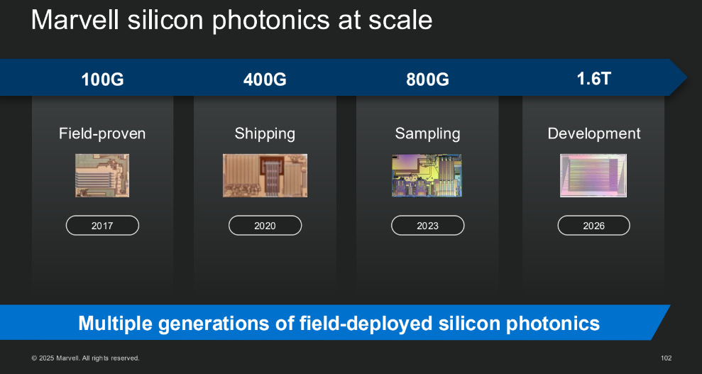
Marvell is driving the deployment of 6.4T and 1.6T silicon photonic engines, combining low power and high-density integration to support the rise of Co-Packaged Optics (CPO) and Linear Pluggable Optics (LPO) in hyperscale data centers.

In intelligent optical processing, companies like NewPhotonics and Celestial AI are pioneering DSP-free architectures with their Optical Signal Processor (OSP) technologies and advanced packaging (e.g., OMIB), enabling ultra-low-latency optical paths tailored for AI-native infrastructure.

Meanwhile, Drut Technologies is defining the emerging fabric of chiplet-to-chiplet optical interconnects using silicon photonics, unlocking disaggregated memory-compute architectures that are crucial for next-generation CXL and AI/ML systems.

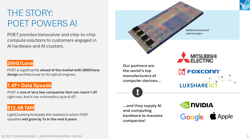
On the packaging front, POET Technologies introduces a passive-alignment Optical Interposer™ platform that integrates flip-chip lasers with hybrid PIC/EIC structures, offering cost-effective photonic engines for edge applications and AI workloads.
Most critically, in the often-overlooked domain of electro-optical co-testing, the trio of TSMC, NVIDIA, and ficonTEC is establishing foundational infrastructure. Among them, ficonTEC plays a pivotal role by delivering the world’s first 300mm double-sided wafer test platform, seamlessly integrating automated electro-optical alignment, active optical probing, and high-throughput test flows. Their system allows for concurrent electrical and photonic characterization at the wafer level, an essential capability for validating the performance and yield of high-speed optical engines in real manufacturing environments. ficonTEC’s innovations not only de-risk production for CPO and PIC developers, but also help standardize optical test methodologies across the industry.

2025 Taiwan Semiconductor and Silicon Photonics Industry Summit
Foxconn is a key partner of NVIDIA and has been deeply engaged in the development of silicon photonics. Its research institute brings rich experience across industrial applications, academic research, and practical implementation. In particular, optical and electrical testing is a critical step in ensuring the quality and reliability of photonic chips and wafers.
Foxconn Research Institute

The Foxconn Research Institute serves as the core innovation engine driving the Foxconn Technology Group’s transformation and upgrade. It focuses on disruptive technologies expected to shape the next 3 to 7 years, including semiconductor processes, AI computing, robotics systems, and electric vehicle platforms.
In the semiconductor domain, the institute adopts an application-driven approach—working backward from system-level needs to materials and processes. It emphasizes innovation across advanced packaging, thermal management, optoelectronic integration, and AI chip platforms, thereby strengthening Foxconn’s capabilities in next-generation data centers and smart manufacturing.
Recently, ficonTEC introduced an innovative Optical Engine Double-Sided Testing solution — a 300?mm wafer-level testing platform designed for co-packaged optics (CPO). This system supports ATE (Automatic Test Equipment) frameworks and is equipped with six-axis optical alignment, high-speed electro-optical measurements, automated calibration, and thermal control. It significantly enhances the efficiency and yield of CPO device production.

In Taiwan, semiconductor giants such as TSMC, ASE, and SPIL are actively participating in the silicon photonics ecosystem — from fabrication to packaging and testing — forming a comprehensive and competitive supply chain. TSMC, in particular, is expected to apply its SoIC (System on Integrated Chips) and advanced packaging technologies to integrated photonic-electronic solutions.

- Date & Venue: September 2025, at TaiNEX (Taipei Nangang Exhibition Center), held in conjunction with SEMICON Taiwan.
- Key Highlights:
- The SEMI Silicon Photonics Forum will feature leading experts from the fields of photonic integration and advanced packaging, including senior executives from TSMC.
- Topics will include cutting-edge optical-electrical measurement, double-sided wafer testing, and mass production strategies.
- Industry leaders from powerful companies, and Taiwan’s semiconductor supply chain will share their latest innovations and field insights.
- September marks not only SEMICON Taiwan’s peak season but also a key moment for Taiwan’s global role in the silicon photonics value chain.
Why You Shouldn’t Miss This Event
- Technology Leadership: ficonTEC’s double-sided wafer test platform is an industry-first and has been adopted by major ATE vendors like Teradyne.
- Robust Ecosystem: Taiwan’s TSMC, ASE, SPIL, and others lead in silicon photonics manufacturing, packaging, and testing.
- Networking Opportunities: Meet and exchange with industry leaders, academic experts, and innovators at the forefront of photonics and semiconductors.
- Market Momentum: Driven by AI and CPO applications, the silicon photonics market is undergoing explosive growth, enabling the future of high-speed interconnects, data centers, and HPC.
You’re Invited:
Join us in Taipei this September for one of the most important semiconductor and silicon photonics gatherings of the year. Witness the latest technology breakthroughs, supply chain collaborations, and industry-defining trends. Don’t miss the chance to engage with global innovators and shape the next wave of photonic integration.
For agenda details, registration, or speaker updates, please follow SEMI Taiwan’s official website and press releases.
Final Note: This September, Taipei is more than just the global stage for semiconductors — it’s where the future of silicon photonics comes into focus. We look forward to seeing you at this landmark event!
Together, these companies—spanning design, packaging, testing, and interconnect—represent the critical ecosystem driving photonics from innovation to implementation. As the industry moves toward modular, scalable, and power-efficient systems, their technologies form the backbone of the coming wave of optical infrastructure.
As the industry rapidly deploys across various technological domains of optoelectronic integration—from Marvell’s high-bandwidth photonic engines, NewPhotonics and Celestial AI’s AI-native optical signal processing, to Drut and POET’s breakthroughs in die-to-die interconnects and optical interposers—the entire supply chain is accelerating toward modularity, low power consumption, and scalability. Amid this technological surge, AIM Photonics is increasingly emerging as a pivotal driver.
Supported by the U.S. Department of Defense as a manufacturing innovation platform, AIM Photonics provides a comprehensive implementation environment for photonic processes, packaging, and interposer design. More critically, it integrates numerous key enterprises and research institutions, such as GlobalFoundries, Analog Photonics, and NIST, to establish a reproducible, verifiable, and scalable hub for heterogeneous integration innovation. From wafer-level photonic manufacturing and double-sided electro-optic testing platforms to standardized PDK/ADK design support, AIM Photonics is forging a “photonics highway” that rapidly translates innovation into applications. At this critical juncture in the global race to realize next-generation optoelectronic systems, AIM Photonics serves not only as a technology enabler but also as a catalyst and central hub for system integration, bridging the gap from concept to implementation in the photonics industry.
As artificial intelligence, quantum computing, and high-speed communications continue to reshape the global infrastructure landscape, photonic integrated circuits (PICs) have evolved far beyond their origins as lab-scale prototypes. Today, they are becoming essential engines for the next generation of data processing and interconnect performance. Yet despite this progress, the PIC industry has long lacked a truly integrated, end-to-end platform capable of bridging the gap between design, manufacturing, packaging, and testing to support full commercial deployment. The emergence of AIM Photonics fills this structural void.
Backed by the U.S. government as a national manufacturing innovation institute, AIM Photonics offers not only best-in-class 300 mm wafer-based photonic manufacturing but also integrates interposer design, advanced packaging, pluggable optical coupling, and electronic-photonic design automation. This comprehensive ecosystem enables startups and global enterprises alike—across quantum research, AI acceleration, and beyond—to access the infrastructure needed to realize complex photonic systems. More than just a foundry, AIM serves as a strategic innovation engine catalyzing the industrial transformation of integrated photonics.
In an era where the scale and complexity of AI systems are expanding exponentially, traditional electrical interconnects are approaching physical and energy-efficiency limits. To break through these bottlenecks and unlock system-level performance gains, photonics and co-packaged optics (CPO) are rapidly becoming mainstream. This is not merely an interconnect revolution—it marks a fundamental shift in heterogeneous integration and advanced system packaging. At the IEEE HIR Workshop, industry leaders and technical experts will explore one central question: what role will photonics and CPO play in shaping the AI infrastructure of tomorrow?

Introduction to AIM Photonics:
AIM Photonics (American Institute for Manufacturing Integrated Photonics) is a U.S. national innovation institute dedicated to the development of next-generation integrated photonics manufacturing and advanced packaging solutions. Established under the framework of the U.S. government’s manufacturing innovation initiative, AIM Photonics is headquartered in New York State and led by SUNY Polytechnic Institute. It brings together a broad coalition of industry, academia, and research institutions to build a comprehensive silicon photonics technology ecosystem.

AIM Photonics not only provides PDKs (Process Design Kits), testing, and fabrication platforms, but also actively promotes a complete workflow from design and wafer manufacturing to advanced packaging. Its core mission is to accelerate the adoption of photonic-electronic integration in applications such as data centers, defense, healthcare, and quantum computing. As a key participant in the ECTC conference’s discussions on CPO and AI system integration, AIM Photonics stands at a pivotal juncture in the global photonics industry.

Overview of AIM Photonics Platform: End-to-End Photonic-Electronic Integration Services
- Design Enablement
AIM Photonics offers comprehensive Process Design Kits (PDKs), featuring over 80 components including waveguides, photodetectors, and modulators. These PDKs are compatible with leading EPDA tools such as Synopsys and Cadence.
In addition, the platform provides extended Assembly Design Kits (ADKs) and Measurement Design Kits (MDKs) to support packaging and testing design, ensuring reliability and consistency from concept to realization.
- Multi-Project Wafer (MPW) and Interposer Wafer Services
Built on the world’s first 300?mm silicon photonics integration platform, AIM’s MPW service enables cost-effective and rapid prototyping through shared wafer production.
The platform supports a wide range of photonic integrated circuit (PIC) processes, including active, passive, low-loss, high-sensitivity sensing, and Quantum Flex (QFlex) options.
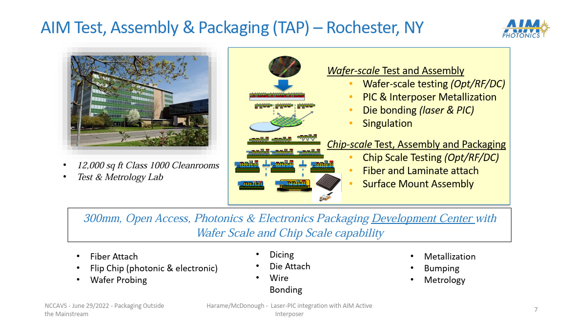
Manufacturing and testing take place at two core facilities: the NY CREATES 300?mm fab in Albany and the TAP testing and packaging center in Rochester.
- Testing, Assembly, and Packaging (TAP)
The Rochester TAP facility is the world’s only open-access 300?mm packaging development platform, supporting photonic-electronic integration, laser co-packaging, and chip-to-chip optical interconnects.
It promotes reusable design templates (e.g., PDK v1.0) and supports advanced co-design including laser chip integration, complementary interface design, thermal management, TSV/RDL, and more.
- Education and Workforce Development
AIM offers both online and in-person courses, summer camps, internships, and photonics workshops to train cross-disciplinary talent in PIC design, manufacturing, and testing.
From FY20 to FY24, its educational programs engaged over 11,000 participants in collaboration with more than 107 organizations.
- Strategic Positioning and National Impact
As one of the eight manufacturing innovation institutes established by the U.S. Department of Defense (DoD), AIM Photonics is jointly supported by federal and New York State funding and operated by SUNY.
The platform significantly reduces prototyping costs—by an estimated 80–90%—while accelerating U.S. photonics industry deployment and supply chain development.
Its R&D focus spans telecom/data center interconnects, RF/microwave photonics, sensing and LiDAR, and quantum photonics.
Platform Value Summary
- Comprehensive Development Chain: A true end-to-end ecosystem covering design ? fabrication ? packaging ? testing across the full PIC lifecycle.
- Low-Barrier Prototyping: The 300?mm MPW service dramatically lowers both risk and cost for photonic prototyping.
- Predictable and Efficient: The combination of PDK + ADK + MDK enhances design manufacturability and shortens R&D cycles.
- National Security & Economic Competitiveness: Strengthens U.S. autonomy and leadership in photonic manufacturing technologies.
|


