Yes—ASML’s eScan 2200 and eP6 tools are poised to significantly boost EUV productivity by improving defect detection, metrology precision, and throughput, especially for High-NA EUV nodes. These tools reduce mask and wafer rework, enabling faster ramp and better yield.
Here’s how each contributes:
eScan 2200: Multi-Beam Wafer Inspection
- Purpose: High-throughput e-beam inspection for EUV-patterned wafers
- Key Impact:
- Uses multi-beam architecture to inspect wafers up to 100× faster than single-beam tools
- Targets physical defects at sub-2nm nodes, including stochastic failures and line-edge roughness
- Enables inline defect monitoring, reducing cycle time and improving yield
- Productivity Boost:
- Cuts inspection bottlenecks for EUV layers
- Supports early ramp of High-NA EUV by catching defects before costly rework
eP6: High-Resolution SEM Metrology
- Purpose: Critical dimension (CD), edge placement error (EPE), and overlay metrology for shrinking nodes
- Key Specs:
- Resolution: 1.5 nm (vs 1.8 nm for eP5)
- Precision: 0.07 nm (vs 0.1 nm)
- Distortion: 0.25 nm (vs 0.8 nm)
- Throughput: ~2× faster image acquisition than eP5
- Productivity Boost:
- Enables accurate process control for High-NA EUV and thin resist stacks
- Reduces systematic metrology errors, improving overlay and CDU (critical dimension uniformity)
Strategic Impact
- High-NA EUV ramp: Both tools are essential for 0.55 NA scanners, where tighter specs and stochastic variability demand better inspection and metrology.
- Yield acceleration: Early defect detection and precise metrology reduce rework and scrap.
- Energy efficiency: Fewer re-spins and better process control reduce overall energy per wafer.
These tools aren’t just incremental—they’re foundational for scaling EUV beyond 2nm. If you want to compare eScan 2200’s multi-beam layout to Applied’s ColdScan or KLA’s Gen5 e-beam roadmap, I can break that down too.
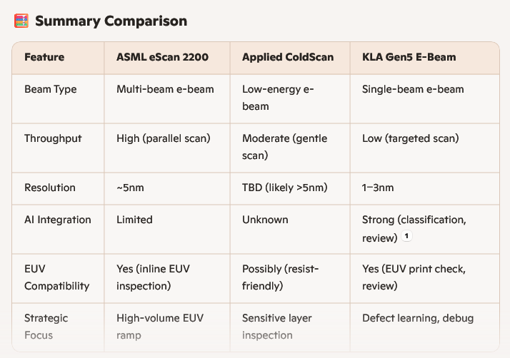
ASML’s eScan 2200 uses a multi-beam architecture for high-throughput EUV wafer inspection, while Applied’s ColdScan and KLA’s Gen5 e-beam systems take different paths—ColdScan focuses on low-energy defect detection, and KLA emphasizes single-beam precision with AI-enhanced classification. Each has trade-offs in speed, resolution, and integration.
Here’s a breakdown of how they compare:
ASML eScan 2200: Multi-Beam Wafer Inspection
- Architecture: Multi-beam e-beam system with dozens of parallel beams scanning simultaneously
- Strengths:
- Throughput: Up to 100× faster than single-beam systems
- Resolution: Sub-5nm defect detection, tuned for EUV layers
- Use Case: Inline inspection of EUV-patterned wafers, especially for High-NA ramp
- Challenges:
- Beam calibration complexity
- Stitching artifacts between beamlets
- Strategic Role: Enables early defect detection for sub-2nm nodes, reducing rework and improving yield
Applied Materials ColdScan
- Architecture: Low-energy e-beam inspection platform (still under wraps, limited public specs)
- Strengths:
- Gentle inspection: Reduces resist damage and charging effects
- Targeted Use: May focus on voltage contrast or buried defect detection
- Challenges:
- Lower resolution than high-voltage e-beam
- Throughput not yet benchmarked publicly
- Strategic Role: Complements optical and high-voltage e-beam tools for sensitive layers
KLA Gen5 E-Beam (eSL10, eDR7380)
- Architecture: High-resolution single-beam systems with AI-driven classification
- Strengths:
- Resolution: 1–3nm defect sensitivity
- AI Integration: Reduces false positives to <3% without hardware changes
- Use Case: Hotspot inspection, electrical defect review, process debug
- Challenges:
- Throughput: Slower than multi-beam systems
- Coverage: Best for targeted inspection, not full-wafer scans
- Strategic Role: Precision tool for yield learning and defect root cause analysis
 |


