TSMC: 5nm on Track for Q2 2020 HVM, Will Ramp Faster Than 7nm
anandtech.com
TSMC’s 5 nm (N5) manufacturing technology is projected to provide significant benefits when it comes to performance, power, and area scaling, which is why the contract maker of semiconductors expects a tangible number of its customers to adopt this process. And, with a forecast for aggressive demand paired with some early preparation in installing new equipment, TSMC believes that its N5 technology will ramp even quicker than its 7 nm (N7) process.
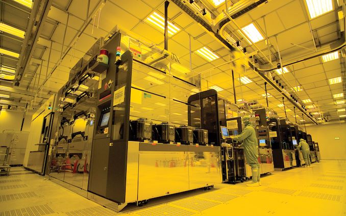
In a bid to boost its production capacities, TSMC recently increased its capital expenditures for 2019 from $10 billion - $11 billion to $14 billion - $15 billion. TSMC is particularly invested in buying equipment for its cutting-edge nodes, such as ASML’s Twinscan NXE step-and-scan systems for processes that use extreme ultraviolet lithography (EUVL) for select layers. At present, TSMC’s Fab 15 is making SoCs using N7+, whereas its Fab 18 (the first phase of equipment move-in was completed in March 2019) is on-track to produce N5 chips in high volume starting Q2 2020.
AdChoices
ADVERTISING
The new tools that will be bought in the coming months are expected to be installed in 2020 and this is when the company will be able to quickly ramp production of chips using its N7, N7+, N7P, N6, N5, and N5P process technologies. The company is confident that it will have a very high market share with its 5 nm nodes.
Volume 0%
Press shift question mark to access a list of keyboard shortcuts
Keyboard Shortcuts
Play/PauseSPACE
Increase Volume?
Decrease Volume?
Seek Forward?
Seek Backward?
Captions On/Offc
Fullscreen/Exit Fullscreenf
Mute/Unmutem
Seek %0-9
C.C. Wei, vice chairman and CEO of TSMC, said the following:
First, the 5 nm ramp for next year. Certainly, as compared with six months ago, we are right now more aggressive and more optimistic about it. Hopefully, because we spend big money [...] that it will ramp up much in terms of revenue, be much faster than 7 nm. […] With that money, we spend to buy the tools to prepare everything. We do expect that our growth will go beyond 5% to 10%.
The key difference between N5 and its predecessors that use EUVL is that it is designed to use EUVL on up to 14 layers (up from four and five in case of N7+ and N6). So the ramp of N5 will increase usage of the latest equipment, and to some degree will demonstrate whether EUV tools and ecosystem is ready for prime time or not. Right now, TSMC seems to be very optimistic about EUVL. The light sources it uses offer output power of more than 250 Watts and reach target goals for availability. The company also produces its own pellicles and takes into account characteristics of currently available photoresists.
Mr. Wei said the following:
“We produce our own pellicle. We have a large number of masking capacity and everything. So even photoresist, those kind of things, we have been taking into account. We are in a high-volume production [with] EUV lithography technology. For next year, you have big — even higher volume, and I can assure you that we are all prepared.”
Related Reading:
Source: TSMC |


