Of the four entities designing 3D NAND, three took a relatively similar approach (using charge-trap technology), and one took an entirely different approach - the IMFT (IM hereafter) partners Intel and Micron. Not only did IM stay with floating gate, it was the only one to utilize "logic on the bottom" of the die memory array. This approach promised three major advantages over any of the other suppliers' approaches. First, staying with floating gate would possibly give it a learning curve advantage. This is because IM (as had all the other suppliers) used this approach with its previous planar NAND generations. "Stay with what you know" is the philosophy here, but would it prove out in greater yields? Beyond this, the second and probably more important reason for staying with floating gate is that it would enable the IM partners to design a higher quality, more robust die that would be much more reliable and durable than competing 3D NAND designs. Finally, logic on the bottom promised to give IM a cost advantage, in that this approach allowed IM to design a die with greater bit density since it would not be subject to the 30% of die area penalty that logic on the side imposed.
Here's a slide from Micron 2015 Summer Analyst Conference that sums up Micron's positioning:
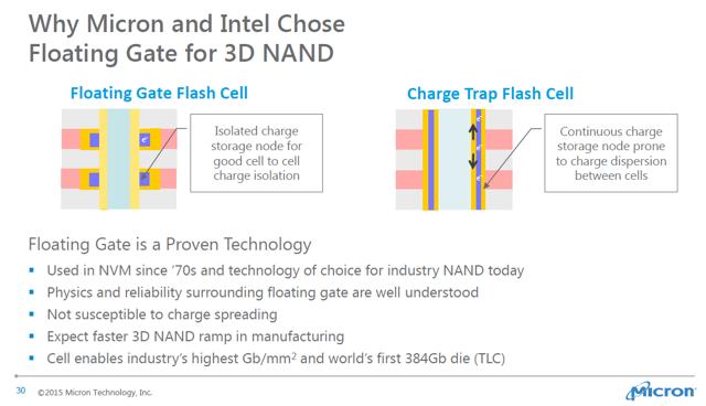 Click to enlarge Click to enlarge
The upshot of this approach? If it worked out, the IM partners would come to market with a technology process that scaled faster and more economically and was of higher quality. Put another way, IM's 3D NAND process would provide more 3D bits sooner at less cost and of higher quality than other suppliers. But where is the evidence that IM achieved its goals?
For part of the answer, we need look no further than the WDC concall. Here is Mike Cordano (president and COO) forecasting WDC's 3D bit output goals in FY (CY) 2017.
"Given the planned mix of 2D and 3D NAND technologies, for the rest of the year we expect our bit supply growth to be approximately 30% in calendar 2016, somewhat below our estimate for total industry bit supply growth, as we had previously indicated. However, as we look to 2017, the planned rate of conversion of our 2D NAND capacity to BiCS3 will enable a mix of our 3D NAND wafer capacity to approach 40% of the total capacity by the end of 2017. This will place both our mix of 3D NAND capacity and our overall bit growth rate in line with the industry." - SA Transcripts (emphasis by author) WDC Q4 Concall
Note the "approach 40%" language. Let's now turn to cost, which is closely associated with density. Here is Steve Milligan (CEO) discussing their strategy for introducing the BiCS3 process node (BiCS3 is WDC's 64L 256Gb TLC die).
"... we want to manage technology transitions when it makes sense from a cost standpoint. So it, right now, we have the leading 2D planar technology from a cost standpoint. So we want to intersect 3D NAND technology when we think it is cost competitive to the incumbent 2D NAND technology. We believe that that will occur with our BiCS3 technology […] with 64 layers, that's where we believe that cost crossover point will begin to occur, and we'll be ramping accordingly when that takes place through 2017." - SA Transcripts (emphasis by author) WDC Q4 Concall
So what is WDC telling us with this information? First off, that it is being consistent with what Sanjay Mehrotra (former CEO of SanDisk) has been saying for at least the last two years, and that is that 2018 will be the first year that 3D bit output exceeds planar. Micron, in contrast, will exit this calendar year with 3D bit output as the majority of its NAND bits starting in the late fall. So we're talking about Micron having a full-year advantage in ramping 3D bits over WDC. This is very important because of the cost advantage implications for the IM partners.
Now, it is true that Cordano is talking wafers, and Micron is talking bits. Is it possible that its Gen 3 BiCS3 die will be so dense that the 40% of the wafers producing 3D bits can outproduce the 60% of the wafers producing the 15nm planar bits? We can't be sure because WDC has yet to give us that data, but we do know that bit density and yield combine to generate cost per bit. Note Milligan's language above - "We believe that cost crossover will begin to occur". This tells me that however dense its new 64L die is, it's going to take a while for WDC's 3D NAND bit output to reflect it. Given this fact, I'm modeling only a 10% effective density gain in 2017 until we get more definitive information. Bottom line, at 10% greater effective density, we project that WDC 3D bit shipments will not pass 50% until well into 2018.
Contrast this with Micron's 32L 384Gb TLC die, which MU has been positioned as 25% less expensive than its 16nm planar offering, which in turn is roughly comparable in cost to WDC's 15nm planar. Let's give WDC a 10% cost advantage with its smaller 15nm process, but in any case, MU likely has at the very least a cost advantage over the BiCS3 die with its 32L TLC process. The bottom line - Micron's 32L TLC process is producing more 3D bits at less cost than WDC, and only slightly less than the FF partners altogether, despite FF having roughly 40% of the industry's total wafer output. Advantage Micron.
There's more. Micron is on schedule with its Gen 2 die that is coming to market in 2017 at an additional 30% cost reduction. Here's what Micron had to say at its 2016 Winter Analyst Meeting regarding cost and production timing of its leading-edge NAND process.
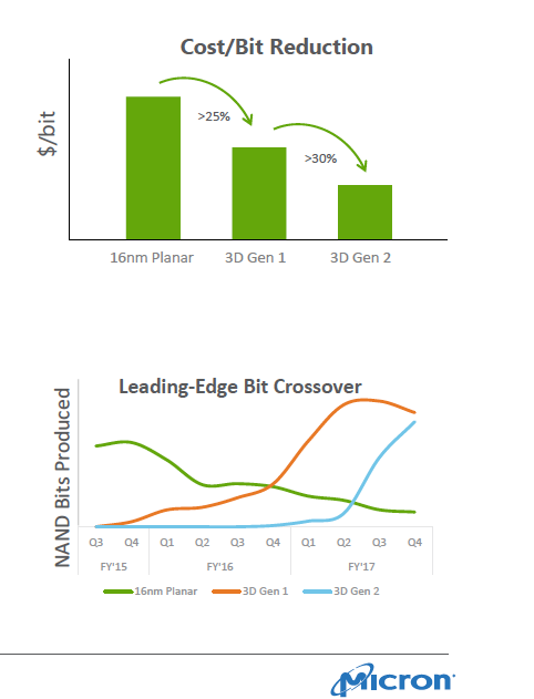
Take a hard look at the bottom slide. Micron will be generating between 30% and 40% of its bits by September of next year in the Gen 2 node. This node is widely rumored to be a 64L 768Gb TLC node. Look at the two lines that represent Gen 1 and Gen 2 3D compared to Micron's planar output as of the end of Micron's fiscal year in August 2017. Note also that the Gen 2 node output is accelerating rapidly as calendar year-end approaches.
The conclusion? Micron will be a full year ahead of Western in converting to a higher quality, more robust, and more desirable product with all these attributes coming at a cost that is likely to be 20% to 30% below the corresponding WDC product. And the competitive advantages of having more 3D product should not be underestimated.
seekingalpha.com |


