AMSL: 4.5 Million Cumulative EUV Wafers Processed Through 2018
tomshardware.com
(...)
ASML has disclosed at the IEDM 2019 conference that a total of 4.5 million wafers had been processed using EUV tools until 2019, as reported by AnandTech. The company’s latest NXE:3400C systems achieves 170 wafer per hour throughput.
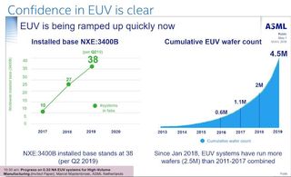
Of the 4.5 million wafers that had cumulatively run through ASML’s EUV tools from 2011 until late 2018, the majority (2.5 million) occurred in 2018 alone, roughly doubling each year since the 0.6 million at the start of 2016. For comparison, TSMC manufactures roughly 12 million wafers annually, although it should be noted that a wafer undergoes potentially dozen of lithography exposures during its manufacturing.
The number of wafers processed by EUV has likely risen even more in 2019, as both Samsung and TSMC have started production of their 7nm and N7+ processes. Chips based on EUV include the Samsung Exynos 9825, Kirin 990 5G, and next year, Qualcomm’s 5G Snapdragon chipsets and AMD’s Zen 3. Intel will adopt EUV in 2021 with 7nm.
The installed base of the NXE:3400B systems reached 38 as of the second quarter of 2018, almost quadruple the amount of 2017. It shows that EUV adoption is growing and customers have confidence in the technology: ASML received 23 EUV orders in the third quarter of 2019 (and stated that it would deliver ~35 systems in 2020), including several systems for DRAM. All those orders were for the new NXE:3400C system that also started shipping in the third quarter.
NXE:3400C Update
(Image credit: AnandTech)Despite EUV being even more delayed than Intel’s 10nm process, ASML highlighted the progress it has made on EUV throughput, the main factor that has limited its economical viability. This has increased by over 17x in five years. The latest NXE:3400C achieves a 170 wafers per hour. Throughput in commercial deployments will likely be lower, though, based on the exposure dose and system downtime.
(Image credit: AnandTech)Another improvement to the NXE:3400C has been its modular vessel, which improves serviceability to reduce the mean time to repair (MTTR) significantly to improve its availability metric, which has reached 75% to 85%, according to AnandTech.
(Image credit: AnandTech)The throughput and availability metrics show EUV's steady progress towards commercial viability over the year.
The NXE:3400C will be followed by the EXE:5000 series in 2023 with a 0.55 numerical aperture (NA) compared to the former’s 0.33NA, improving the resolution by 67% and the effective wafer throughput by even more compared to multiple patterning EUV on a 0.33NA system. |


