Intel finally tells it like it is:
"Look, [10nm] isn't going to be the best node that Intel has ever had. It's going to be less productive than 14nm, less productive than 22nm. But we're excited about the improvements that we're seeing, and we expect to start the 7nm period with a much better profile of performance, starting at the end of 2021 […] we feel like we're starting to see the acceleration on the process side […] to get back to parity in the 7nm generation and regain leadership in the 5nm generation."
tomshardware.com

So it looks like AMD has a process advantage until 2022 at least.
Meanwhile TSMC announces new advances for their CoWoS packaging technology:
TSMC's New CoWoS Tech Doubles Memory Bandwidth
"TSMC announced a partnership with Broadcom to introduce an enhanced Chip-on-Wafer-on-Substrate (CoWoS) platform, a 2.5D integrated circuit (2.5D IC) through-silicon via (TSV) interposer-based packaging technology, that supports the industry’s first and largest full 2x reticle size interposer. The next generation CoWoS interposer has an area of approximately 1,700mm2 and can be used to boost computing power for high-performance computing (HPC) systems. The technology will also be ready to support TSMC’s next-generation 5nm process node. The new CoWoS generation can accommodate multiple logic system-on-a-chip (SoC) dies and up to six cubes of high-bandwidth memory (HBM) supporting up to 96GB of memory. The new CoWoS technology also provides 2.7 terabytes per second (TB/s) bandwidth, which is 2.7x higher than TSMC’s previous CoWoS technology that it launched in 2016. TSMC also says the interposer provides 2.2X more memory bandwidth than any other competing technology."
tomshardware.com
TSMC Announces 2x Reticle CoWoS For Next-Gen 5nm HPC Applications
"TSMC continuously improves its Chip-on-Wafer-on-Substrate (CoWoS) technology. Today, the company is announcing that, through a collaboration with Broadcom, it is introducing an enhanced CoWoS packaging technology supporting the full 2x reticle size interposers, the largest announced to date. As part of the collaboration, Broadcom defined the top-die, interposer, and HBM configuration while TSMC developed the packaging manufacturing process. With the current i193 and EUV lithography steppers, you are looking at a maximum reticle field size of 26 mm by 33 mm or 858 mm². The new CoWoS enhancement enables chips up to around 1716 mm² in order to enable the larger HPC applications such as HBM-based CPUs and GPUs. TSMC says that the new CoWoS packaging technology is being ready to support its upcoming 5-nanometer node."
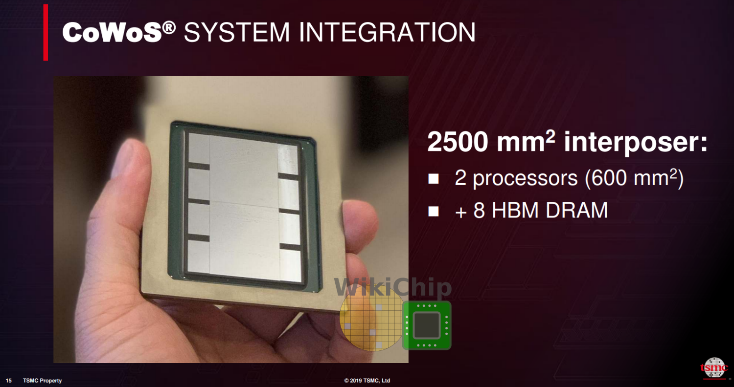
"Looking a little further, TSMC has plans for even larger interposers with up to 3x the reticle size or even larger. At three times the reticle, this means interposers of up to 2574 mm². Last year the company showed off a massive 7.5 x 7.5 cm² package with two large 600 mm² dies along with eight stacks of HBM memory. No word on when we can expect the technology to make it to market."
fuse.wikichip.org
 |


