The Conductive Ink Market By David Savastano, Editor | 03.07.17
The flexible and printed electronics market is gaining traction.
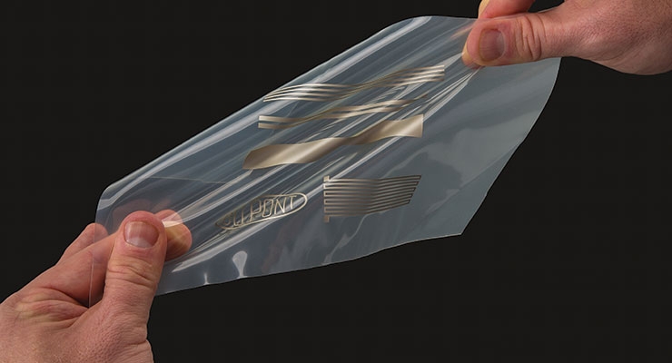
Photo courtesy of DuPont.
The flexible and printed electronics market is quickly finding new commercial opportunities, and conductive inks are evolving to meet these needs. The market for conductive inks and pastes is a $2 billion business, and there is likely more growth to come in areas such as in-mold inks and stretchable inks, among others.
Currently, solar cells are the largest consumers of conductive inks and pastes, and Dr. Khasha Ghaffarzadeh, research director for IDTechEx, sees that continuing in the coming years.
“Solar remains the largest volume market for conductive inks and pastes and will remain so for the foreseeable future,” said Dr. Ghaffarzadeh. “In particular, there is a lot of activity in China as people are installing solar panels before feeding tariffs come to an end. That means good business for paste suppliers and even powder suppliers.”
Roy Bjorlin, global commercial & strategic initiatives director, Sun Chemical Advanced Materials, noted that the smart packaging field is drawing a lot of attention from brand owners.
“There is a lot of curiosity towards electronic packaging and smart labels, and brand owners are increasingly expressing interest,” Bjorlin said. “The United States and European markets appear to be ahead of the curve, and it is likely that production volumes will grow as the traditional packaging converter base starts developing more manufacturing capabilities for electronics at lower costs. For that to happen, the market also needs to determine which functions are to be implemented. This will be largely determined by a combination of cost and benefit analysis as well as consumer acceptance.”
“Companies are coming to us to help them with getting electrical functionality onto substrates that are being selected because of their ability to enable new form factors, and because of new application criteria,” said Stan Farnsworth, VP of marketing for NovaCentrix. “This need is common throughout the emerging application areas of wearables, IoT, smart packaging and even in automotive, aerospace, and defense. I think the message of printed and flexible electronics enabling new form factors and new functionality is being heard.”
Sarah Wilson, product promotion specialist II at Brewer Science, Inc., said that the flexible and printed electronics field has gained traction in recent years.
“Although the initial growth of the printed electronics industry was not as fast as expected, mainly due to too-high expectations, the printed electronics market appears to have gained momentum,” Wilson observed. “Even before this technology was available on the market, there was great interest and a big push to use these products in various daily commodities such as cell phones, displays, smart wearables, lighting, smart packaging, labels, shipping, storage, etc. We are seeing an increase in potential for the future of flexible sensors along with an increase in higher production volumes and capabilities. Printed electronics products such as printed antennas, RFID tags and sensors have begun to be manufactured with scaled production such as roll-to-roll, and have appeared as commercial products in the market.”
Kerry Adams, printed electronics market segment manager, DuPont, said that the technology is wide reaching across many markets, but DuPont is seeing opportunities in transportation, white goods, wearables, healthcare and consumer electronics applications.
“With trends in mass customization, the proliferation of new brands and the IoT, we believe that printed electronics has a bright future. Labels with printed sensors and means to report environmental and location information are not far away,” said Dr. Daniel Harrison, SVP R&D at IIMAK. “Smart shelf talkers will be enabled with printed electronics to provide customers with detailed information to aid in their purchases.”
“As the innovation continues in the flexible electronics industry and OEMs realize that printed electronics is less of a buzz word and more of a reality, I think we’ll all be impressed with where new applications begin to come from and what products we’ll start to see hitting shelves of the consumer, industrial, military, medical and automotive markets,” said Ryan Banfield, business development specialist for Applied Ink Solutions.
Additive printing, or 3D printing, is another technology for printing conductive inks. Fernando de la Vega, CEO of PV Nano Cell, said that the company’s Sicrys inks are being used in a wide range of applications.
“Our products are being used to create mobile phone parts, touch screens, printed circuit boards and one layer electronics such as sensors as well as photovoltaics. These will soon reach the market,” said de la Vega.
Dr. Ghaffarzadeh observed that ink suppliers are branching out into new markets in order to be ready for any breakthrough applications.
“There are many emerging market frontiers, and the market is very exciting and is changing,”
Dr. Ghaffarzadeh noted. “The story of the conductive ink business is that nobody wants to be left behind. The big players are developing as broad a product portfolio as they can, hoping that one or more of these niche markets become massive success stories. That’s why these companies have all kinds of new inks on the market, whether they are inks that are in-mold compatible, inks that are stretchable, inks that can be used in extremely high or extremely low temperatures or many others. The ability to customize your formulation will be a big selling point.”
For example, Dr. Ghaffarzadeh pointed to in-mold electronics (IME) as an area where there are plenty of opportunities emerging.
“In-mold electronics are one market that is interesting to watch this year,” he said. “It has seen many false starts, but I think that 2017 will be the year that we see some real commercial successes. Conductive inks are the first functional material to be fully compatible, and you can already see that the toolkit for in-mold electronics is already expanding, to include transparent conductive films and maybe sensors. IME is a good story to watch in the coming years. EMI shielding is also turning out be an interesting market for spray coated silver nanoparticle inks.”
“As a provider of both functional and graphic inks for in-mold electronics (IME), Sun Chemical is now offering an ‘IME Full Stack’ where both thermoformable and ‘able-to-be-molded’ graphic inks, conductive and dielectric inks can be supported from a single source,” Bjorlin noted. “Sun Chemical is uniquely positioned to provide both form and function for the burgeoning IME process. IME delivers electronic functionality to the molded part, lighter weight, less expensive manufacturing, and greater durability.”
Stretchable silver inks and pastes are another excellent opportunity.
“If you looked at the market two or three years ago, there were only a few companies offering a stretchable silver paste, but now there are more than 10,” Dr. Ghaffarzadeh observed. “The first generation of stretchable inks demonstrated huge changes in resistance when you stretched them, but now that change is much smaller as formulations have improved. You see many examples where silver lines have been printed on textiles now, often encapsulated to make it washable, and there is an evolution in performance.”
“We have been expanding our portfolio of electronic inks and pastes tremendously over the last two years,” Adams added. “For smart clothing and other wearable electronics applications, we launched a system of stretchable and washable electronic inks.”
Matt Ganslaw, VP, sales for Creative Materials, said that he has seen several projects that have come to fruition recently in flexible medical electrodes, flexible LED lighting, flexible solar cells and RFID antennas.
“The best opportunities for manufacturers in the flexible and printed electronics market is to be working directly with OEMs in the apparel industry who are on the cutting edge of wearables technology,” Ganslaw added. “The primary requirements are stretchability, washability and high abrasion resistance.”
There is plenty of growth for flexible and printed electronics, with more applications emerging. Bjorlin said that the future is bright for intelligent inks and electronic packaging.
“Sun Chemical is confident that advancements in material technology will continue to drive the development of new applications, particularly in the flexible printing space,” Bjorlin concluded.
“Cost drivers in photovoltaics, consumer interest in wearables and smart packaging, and new cost-effective displays and lighting will increase demand for new materials and processes.”
inkworldmagazine.com |


