am watching, and not looking quite good
finance.yahoo.com

bloomberg.com
Intel Inside OhioThe stagnating chipmaker is attempting a comeback with massive spending on new factories and lots of help from the Biden administration.
1 May 2024 at 17:00 GMT+8, Updated on 1 May 2024 at 18:10 GMT+8

Businessweek | The Big Take
By Max Chafkin and Ian King
Photo Illustration by Kelda Van Patten
A few months ago, a tugboat set off from New Orleans, pushing a barge up the Mississippi River. It moved northward through the Deep South and then cut east, past Indiana farmland along the Ohio River. The barge was carrying a cold box for a gigantic air separation unit, a piece of industrial equipment that pulls nitrogen from the atmosphere for use in manufacturing. The cargo was so big that transporting it through Cincinnati, where container ships usually unload in southern Ohio, was impractical. At 270 feet long, 19 feet wide and 24 feet tall, it wouldn’t fit under the highway overpasses near the port. So the boat floated 75 miles or so upriver before stopping at an abandoned dock just outside the tiny village of Manchester. For weeks now, it’s been sitting by the bank, waiting for the final leg of its journey, set to begin later this spring.
Then a team of workers will load the cold box onto a massive semitrailer designed for so-called superloads. While police cars clear the roads between the river and the tower’s destination, cherry-pickers will push power lines and traffic lights out of the way. This convoy-slash-roadblock will proceed at about 8 mph to New Albany, Ohio, stretching out a trip that most cars can make in two hours to about two weeks. Over the next few months, a similar operation will take place 20 more times, delivering air separation and crane parts to a construction site that many in the region are betting will be the future of the semiconductor industry.
This is Ohio One, a future “mega fab”—or factory—being built by Intel Corp. The company has committed $28 billion to build a fab that, if all goes well, will be able to credibly compete for contracts to manufacture state-of-the-art chips used in smartphones and in the training of next-generation artificial intelligence algorithms. Ohio One, says Chief Executive Officer Patrick Gelsinger, could eventually be the biggest chip factory on Earth. Not to be grandiose or anything, he adds, but it’s part of a strategy that will also stave off America’s economic decline, because chips are essential to almost every manufactured good. “I just view this as existential to our economy, to our national security,” Gelsinger says at Intel’s headquarters in Santa Clara, California. “I don’t view failure as an option.”

Gelsinger and Biden breaking ground in Ohio in 2022. Photographer: Gaelen Morse
The fab isn’t scheduled to open until at least 2027, but politicians are already taking credit for even the tiniest bits of progress, posting videos of the superload trips on social media and using every opportunity to talk about the potential job creation. These officials include state Republicansas well as members of the Biden administration, which has made the Intel plant a showpiece for its economic policy. In his State of the Union address two years ago, President Joe Biden called the Ohio One site a “field of dreams,” describing it as “the ground on which America’s future will be built.” This past March the US announced it had agreed to provide Intel with $19.5 billion in loans and grants to help finance the project in Ohio, along with similar ones in Arizona and Oregon, as part of the Chips and Science Act. “Folks, it’s about time,” Biden said, announcing the Intel subsidy package. “Even though we invented the most advanced chips, we make 0% of them today.”
The subtext wasn’t very sub. From war-making to basic communication, the world runs on semiconductors, and most of the best ones are made in Taiwan. In the event of another pandemic or if Beijing decides to invade Taiwan, US supplies of all kinds of hardware could be crippled. In the weeks that followed the announcement of the Chips Act award, there were more subsidies for chip factories in the US: $12 billion for one being built in Arizona by Taiwan Semiconductor Manufacturing Co., better known as TSMC, and $6 billion for one in Texas being built by South Korea’s Samsung Electronics Co. These domestic facilities can’t produce everything the US needs. But while they don’t represent chip independence, they’re at least an insurance policy and, maybe, a start.
Today, Biden’s field of dreams is mostly a muddy expanse on the edge of a pig farm. Still, things are happening. Suppliers are renting real estate, community colleges are spinning up programs to train future semiconductor technicians, and 1,400 workers are digging trenches, laying foundations and pouring concrete for the building itself. That’s the easy part. Semiconductor fab production is arguably the most challenging and expensive act in all of business, a mess of attempts to turn experimental science into mass production.
The Intel One construction site in Licking County, Ohio. If all goes very well, it could one day be the world’s largest semiconductor factory.
Source: Intel Corp.
Two fabs are currently under construction, but there’s room for eight in total on the 1,000-acre site. Intel has said it will put as much as $100 billion into the project if it’s fully built out.
Source: Intel Corp.
If the stakes are high for the US, they may be even higher for Intel. The company that turned the phrase “Silicon Valley” into a metonym for the tech industry, and was one of the world’s largest by market value two decades ago, has been upstaged by TSMC and a raft of chipmakers that outsource the actual making of chips. Nvidia Corp., once a bit player best known to gamers who coveted its graphics cards, is now worth more than $2 trillion, or more than 16 Intels. Sales of Intel’s once-dominant processors are stagnant, its stock has fallen more than 30% this year and is down more than 50% from its peak in early 2020. Its manufacturing, once the crown jewel, is bleeding money. In April, Intel disclosed that the manufacturing operation lost $7 billion last year, with more losses to come.
“Huge numbers, atrocious numbers,” says Gelsinger, a wiry, intense engineer who, at 63, has spent most of his professional life at Intel. But Gelsinger blames those losses on the previous regime. He says that when he took over three years ago, Intel was months away from being sold for parts. Now, he says, the company has embarked on a yearslong plan to restore its dominance, just as it did in the 1990s when it overcame what seemed like insurmountable competition from Japanese chipmakers. “This is gonna be hard, multiyear, heavy, expensive,” he says. On the other hand, he adds, “we’ve done it before.”
At bottom, the modern technology industry requires somebody to figure out a way to arrange tiny electric circuits, known as transistors, onto polished silicon discs. Robert Noyce and Gordon Moore pioneered the process at Fairchild Semiconductor, a company they co-founded in 1957, and industrialized it at Intel, which they started 11 years later. Intel created the first commercial microprocessor, the 4004. The 4004 included about 2,300 transistors, with circuits that were about one-tenth the thickness of a human hair, intricately arranged in a thumbnail-size package with the processing power of a computer that would have once occupied an entire closet. This was done using photolithography, a printing technique in which the silicon disc—a “wafer”—is covered with a light-sensitive material and hit with light, burning an intricate pattern. The process has only gotten more complex. In 1976 the top-of-the-line chip had 29,000 transistors. The first Pentium, released by Intel in 1993, had 3.1 million. The company’s Xeon chips, which enabled the rise of Gmail, Netflix and other cloud computing services, have billions.
Intel has defined itself, and the rest of the industry, largely in terms of this sort of escalating complexity. In 1965, Moore predicted that the number of transistors on a state-of-the-art chip would double every year. Moore himself regarded this prediction as more of a guess—decades later he described it as “wild extrapolation”—but Intel took the idea, which has since become known as Moore’s Law, and helped turn it into something like a Silicon Valley religion. Elon Musk has applied it to batteries for electric cars, Masayoshi Son has employed it as a justification for SoftBank Group Corp.’s wild investments in robotics, and Ray Kurzweil has made it central to his theory that someday we’ll all upload our brains to computers and live forever.
While Moore’s Law has exploded in popularity as a metaphor, its predictive power has weakened. In 2006, Gelsinger, then an Intel senior vice president widely seen as a potential CEO, wrote an essay for an engineering newsletter that declared “the genius lives on,” noting “we see no end to Moore’s Law in the coming decade.” But about this time, developers found they could no longer make a chip twice as efficient by simply doubling its number of transistors. As breakthroughs grew tougher and fab costs rose, the market drove more manufacturers out of the business. This included Intel’s main US competitor, Advanced Micro Devices Inc. (AMD), which eventually outsourced its production of high-end edge chips to TSMC instead. In 2009, Intel announced a reorganization that sidelined Gelsinger, and he left to become chief operating officer at EMC Corp., which makes memory systems for servers.
Gelsinger, who’d joined Intel as an 18-year-old trade school graduate from rural Pennsylvania, hasn’t forgotten how it felt to be pushed aside. He’d been at the company for 30 years and was a mentee of legendary CEO Andrew Grove. “It took me a long time to get over it,” he says, before invoking the five-note jingle that still plays at the end of Intel’s commercials. “I did the Intel Bong as I went to sleep each night, and I didn’t stop doing it for three or four years after I was gone. I wanted to run this place.”
His departure coincided with a series of increasingly dire missteps at Intel. The company passed up the chance to manufacture chips for Apple Inc.’s iPhone and struggled to find a way to break into that market in the years that followed. Rivals that took the job—Samsung and, later, TSMC—rode the smartphone boom and used the cash to chase Moore’s Law. There, too, Intel shrank from a challenge.
“We either get the Chips Act done, or I should build all my factories in Asia”
Intel had worked closely with a Dutch lithography company, ASML Holding NV, to develop an etching technique called extreme ultraviolet lithography. EUV promised to help squeeze the size of the features on a cutting-edge chip down from 14 nanometers to 10nm and eventually to even smaller sizes. (In chips, of course, smaller is better.) But the technique was unproven and expensive, and then-CEO Brian Krzanich attempted a workaround with less advanced machines. Gelsinger now calls this “one of the stupidest decisions that Intel made.” He blames it for delays that left the company a full two generations of chips and several years behind TSMC by 2020. (Krzanich didn’t respond to requests for comment.) These technical setbacks would have lasting damage, as AMD’s Taiwan-made server chips gained market share and as companies like Apple, Google and Amazon cut their purchases of Intel’s chips and designed their own instead, paying TSMC to manufacture them. In 2020 Krzanich’s successor, Bob Swan, suggested Intel might have to give up manufacturing, too.
Global Foundry Market Share, 2023
*Largely revenue Intel generates by making its own chips Source: Compiled by Bloomberg
Gelsinger watched this with a mix of pain and frustration. Intel, he believed, was perhaps six months from a total collapse where “nobody could have saved it,” he says. “We would’ve been exiting technology development, and we would’ve been selling the manufacturing assets at dimes on the dollar.”
At the time, he was running another company, VMware, but he wrote a memo to Intel’s board, urging a radically different strategy. Gelsinger would bet it all on manufacturing, investing billions of dollars on fabs while frantically trying to catch up to TSMC’s most sophisticated manufacturing processes. Intel would enter TSMC’s main business of making chips for other companies—known as the “foundry” model—which would lead to higher volumes and allow it to continue to pursue next-generation research. In February 2021, Intel’s board announced the CEO job was his. “The old Intel is the new Intel,” Gelsinger told a group of Wall Street analysts the following month. “The world needs more semiconductors, and we’re going to step into that gap.”
The comments were meant to evoke nostalgia for the Intel of yore and speak to a new political reality. The supply chain disruptions of the Covid-19 era had crystallized the risks of outsourcing. Prominent Republicans and some Democrats were loudly warning about China’s influence on the tech industry and threat to Taiwan. And Biden had just won the White House promising massive government spending to help rebuild the US industrial base. Gelsinger, adopting a pose that was part patriotic technologist and part cold-hearted capitalist, suggested to lawmakers that the US would need to step up its subsidies or lose a national champion. “We either get the Chips Act done,” he recalls saying, “or I should build all my factories in Asia.”
There was a logic to this, but it sidestepped the role Intel itself had played in the decline of US chipmaking capacity when it ceded technological leadership to TSMC. It arguably understated the challenges of mounting a comeback. Intel’s share price has plummeted because investors worry the company can no longer sell enough chips on its own to build lots of new state-of-the-art factories, and its ability as a foundry is unproven. Gelsinger has disputed this, but the fear is that big foundry customers might wait years before giving Intel a substantial contract, says Matthew Ramsay, a semiconductor analyst at TD Cowen. “Intel is still one of the most, if not the most, strategically important manufacturing companies in the United States,” he says. “But when you look at their track record over the last seven or eight years juxtaposed against the amount of wood-chopping they need to do, it’s going to be hard.”
The first thing you notice when you drive onto the grounds of any fab is the infrastructure: power stations, water treatment plants, storage tanks and a vast thicket of pipes used to bring in the enormous quantities of purified air and water the chipmaking process needs.
Each Intel fab starts with the same basic design, a flat-roofed structure with the main factory on the third floor. This is the clean room, the heart of the operation. It sits above two floors of utilities, ducts and equipment, and one floor below what’s got to be the world’s most powerful HVAC system, an array of fans and filters blowing in ultra-pure air. The floor tiles are perforated, and a huge vacuum system underneath them ensures that the air turns over six times per minute. The air filtration is expensive but necessary. A single particle—a tiny flake of dead skin, a droplet of water from a sneeze—can destroy a $10,000 chip. Bright light applied at the wrong time is bad, too, which is why the rooms are lit a dull yellow.
Intel executives like to boast that their clean rooms are a thousand times cleaner than a hospital operating room. The low light and all the talk of purity can make a visit feel a little cultish, as can the secrecy. Until recently, Intel almost never let outsiders in, and even executives would need special permission. But the promise of almost $20 billion in taxpayer money, and the need to persuade other chipmakers to trust it with their designs, has changed the equation.
Workers walking the Silver Highway in an Intel clean room in Oregon while robots carry chips overhead.
Source: Intel Corp.
The clean room’s air is 1,000 times cleaner than a hospital operating room’s. The air inside the tools that make the chips is even cleaner than that.
Source: Intel Corp.
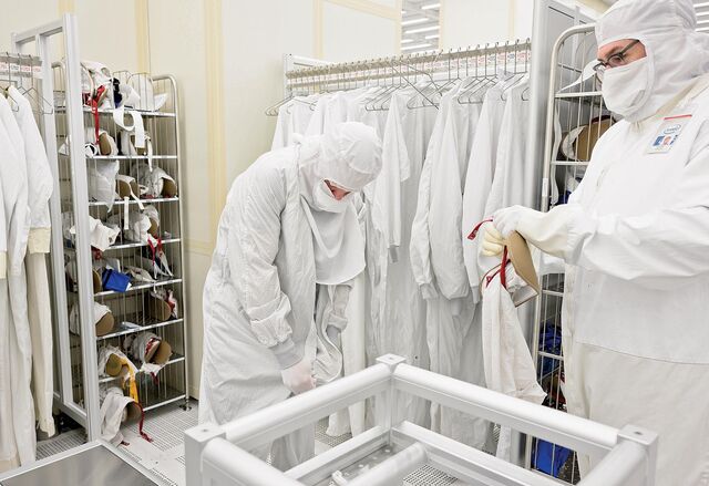
Workers on the floor of an Intel fab must undergo a lengthy “gowning” before they start their day.
Source: Intel Corp.
Intel’s wafers will eventually have hundreds of billions of circuits printed on their surfaces, and will be cut up into hundreds of chips that can sell for more than $10,000 each.
Source: Intel Corp.
In mid-April, a gang of Intel executives and their publicists led two Bloomberg Businessweek reporters through what one guide called a “hierarchy of cleanliness” at D1X, the company’s research and development fab just outside Portland, Oregon. We put on glove liners, hairnets and protective shoe covers. We sanitized our phones with wipes, then turned them off because radio signals can disrupt the machines. That got us into an inner room where we put on hoods with face masks, followed by Gore-Tex coveralls, a second pair of shoe covers, a second pair of gloves and, finally, safety glasses. We were given latex notepads (regular paper sheds particles when written on) and were warned that bumping into anything could risk shutting down production. Then we proceeded, very carefully, through a heavy set of glass doors.
Inside was a space that stretched a dizzying quarter mile long and several hundred feet across. Machines in sizes ranging from large to humongous were laid out on either side of a sort of thoroughfare, a reinforced metal floor known as the Silver Highway. A typical fab has about 1,200 of these “tools,“ which look like distant cousins of the copy machine you’d find in a normal office, only way bigger. A small tool, like a metrology instrument for making sure the layers being deposited on a wafer are properly applied, was the size of a minivan. A medium-size one approximated a school bus.
The largest tool was also the newest: ASML’s latest EUV machine, which is the size of a tennis court and costs $380 million. This “high numerical aperture”—or high NA—EUV machine was positioned in a section of the fab some engineers had taken to calling “the billion-dollar bay,” because of the wildly expensive tools involved. It arrived in Oregon from the Netherlands last year in 43 specially constructed shipping containers. Assembly took months and was only just finished.
Gelsinger says that not long after getting the CEO job he began furiously lobbying ASML for early access to the tool. “It was, you know, ‘We’re not going to debate it, we’re not going to leave this meeting, I’m not going to let you get up from your chair,’?” he recalls saying. For now, he has it: The machine is so new, the only other one that’s fully assembled is at ASML’s own headquarters.
High NA machines are as big as they are because they use light, if you can even call it “light,” that doesn’t occur naturally on Earth, and because they employ an enormous array of mirrors and lenses to shrink the lithography down to a scale that you’d need an electron microscope to see. The light starts just below the fab floor in a huge laser drive—the kind normally used to cut heavy-duty steel. Then it’s shot into three similar laser drives that amplify it further. The laser beam then comes up through a hole in the floor and into the main tool itself. From there, it hits a drop of liquid tin and instantly vaporizes the metal. The tin is heated to 220,000C, about 40 times the surface temperature of the sun, producing a burst of radiation that occurs nowhere in nature.
That extreme ultraviolet light bounces off a series of mirrors before it hits the wafer. The entire operation—the lasers, the tin hotter than the surface of the sun, the mirrors, the wafer—is a single step in a process that takes three to six months to yield a finished product. During that time, each wafer will go through thousands of steps of layering, etching, measuring and washing until there’s an intricate pattern of hundreds of billions of transistors. Some of these layers will be as thin as a single atom. “We build it layer by layer,” says Jeff Birdsall, a vice president who runs manufacturing in Oregon. “Think of it like building a city from the bottom up.” When the wafer is finished, it’s cut into several hundred individual chips.
Suiting up to enter the clean room.

Engineers from ASML work on Intel’s newest tool: a $380 million lithography machine.
Credit: Walden Kirsch/Intel Corp
The obscene cost, complexity and time involved in this microscopic ballet makes sense only if you can do it at high volume, which means having tens of thousands of wafers in production at any given time. But if volume falls, either because customers stop buying or because the process doesn’t work the way it’s supposed to, a chip company can find itself in a sort of death spiral, making less money and then having less to invest in innovations. That’s arguably what’s happening to Intel. As its chipmaking skills declined, it was forced to do what every other chipmaker was doing at the time: outsource its high-end chips to TSMC.
Even today, even with all of Gelsinger’s swagger, roughly 30% of the top-of-the-line chips Intel sells are made by TSMC. Those chips cost Intel extra money to make and they also reduce volumes, making its aging factories even less profitable than they would be. The hope is that by investing in new fabs and by touting state-of-the-art machines, Intel can reverse the death spiral—“bringing more of those wafers home,” as Gelsinger put it in a recent call with analysts. Of course, TSMC and Samsung are also building new fabs and will get their own high NA EUV machines. In fact, just days after Gelsinger talked up his early access to the high NA machine, ASML announced it had shipped one to a second customer. Intel’s head start will last for only a few months.
Building a new fab, on the other hand, takes three to five years, from groundbreaking to full production, and requires some basic elements: “You’re looking at land, power, water,” says Maureen Duhig, an Intel vice president in charge of developing new chipmaking processes. “You need a lot of water.” (Intel’s Ohio site plan called for as much as 6 million gallons a day—roughly twice the volume used by Ohio State University, which has 100,000 students and staff. The company says it will actually use less than that and that most of its water will be recycled.) Then there are the roads, which need to be wide enough to carry all the superloads, not to mention construction equipment and the tools that will eventually be shipped in. Finally, you need people. Fabs are mostly run by robots, but Intel’s project will need thousands of technicians and even more construction workers.
Those potential jobs caught the attention of state governors in early 2021 and led to what Gelsinger describes as an “intense negotiation.” Intel considered bids from four states, including Ohio and Wisconsin, which offered the company a site outside Racine that it had originally set aside for Foxconn, the Taiwan-based contract manufacturer. Gelsinger wouldn’t discuss the failed bids. “You’re negotiating like a thousand line items,” he says. “Are we going to upgrade the sewer? Are you going to upgrade the electrical grid? Are you going to get the transportation systems in? What environmental support are you going to get? It goes on and on.”
Intel accepted Ohio’s bid with a theatrical flourish. “We got this nice white box with a big red ribbon on it,” Gelsinger says. He asked Lieutenant Governor Jon Husted to deliver the package to Governor Mike DeWine that Christmas Day. Intel committed to spending at least $20 billion, employing 7,000 unionized construction workers and eventually hiring 3,000 of its own employees. In return, it got plenty: $600 million in grants for the building, $500 million for roads and other infrastructure, $300 million for a water recycling plant, $650 million in tax breaks and $150 million for employee training. Intel also wouldn’t pay local property taxes on its buildings for 30 years. The project was code-named Cardinal, after the state bird.
In Ohio, Intel promised to hire 7,000 construction workers and 3,000 employees and spend at least $20 billion
In other political environments, more than $2 billion in subsidies for an enormous union-backed construction project might have generated suggestions that this was a waste of public funds, especially from Republicans. But DeWine and Husted won reelection the following November by 15 points, an increase of more than 10 points over their margin in the previous cycle. Meanwhile, instead of mounting opposition, state Democrats mostly tried to claim credit for their part in the agreement, portraying the deal as a vindication of their efforts to bring industrial jobs back to the state. “We are burying the term ‘Rust Belt,’?” Senator Sherrod Brown said at the groundbreaking, calling the factory part of “a new pro-American, pro-union industrial policy.”
Intel has other fabs in the works as part of Gelsinger’s expansion, including two new ones in Chandler, Arizona, and a renovation at D1X that will include an additional fab. But the Ohio project is in some ways the most audacious. It will be the first semiconductor plant in the Midwest and the first time in more than 40 years that Intel has built one of these from scratch, without any existing infrastructure or pools of potential workers nearby. “In Arizona, you already have base facilities, stuff you can work from,” says Jim Evers, the Ohio general manager. “Here, everything’s coming from the ground up. In the first year we had to, like, lay out dirt.”
Last fall, Evers, who wore an Intel work shirt embroidered with “Jimbo,” drove out to the site with a Businessweek reporter. As we set out from the company’s offices, we passed farmhouses, cornfields and a collection of electric transmission towers. “Lots of big lines,” Evers said with admiration, before noting the luxurious width of the country highway we were on. Then he rattled off a litany of recent improvements provided by Intel’s generous hosts: new curbs, new water lines, new storm pipes, new manholes. The site itself was muddy and flat, and, at 1,000 acres, seemed almost endless. We passed a concrete plant, followed by a line of maybe 20 cement mixers, an enormous group of dump trucks and a collection of trailers serving as offices. Farther on, we could see the silos owned by the neighboring pig farm and 10 or so large cranes that hung over a hole where the first fab would be.
Workers had dug a sort of basement level, from which a large collection of columns and pipes had already sprouted. A concrete slab would go over that, followed by two levels of subfab, followed by the clean room itself. Evers noted that the cranes overhead, which had a capacity of 30,000 pounds each, might look big but they were actually sort of puny by Intel standards. “These are not the big crane,” he said. “In fact, they’re not even big enough to put the big crane together.” The big crane—a Liebherr LR 12500-1.0 crawler crane (capacity: 5 million-plus pounds)—will arrive this summer. Intel will use it to mount a collection of enormous steel trusses that form the ceiling of the clean room.
The trusses are necessary because Intel wants its clean room to be a giant unbroken space for the giant and extremely delicate tools. (“Columns just get in the way,” says Mark Phillips, Intel’s director of lithography.) The trusses, which weigh more than 300,000 pounds each and look like the product of the world’s largest erector set, must be strong enough to support a new ASML machine because it will have to be lifted into place from yet another crane attached to the ceiling. After the ceiling is constructed, the clean room will be sealed and filled with filtered air, and then the equipment will start to arrive. In Arizona, that’s happening now. It’s unclear when it’ll happen in Ohio, in part because when you’re building a fab the tools are the most expensive part. “About 25% of the investment is the building, 75% is the equipment,” Gelsinger says. “So I’m going to be pretty confident that the market is there.”
It’s far from guaranteed that the market is waiting on Intel. In February the company announced a deal to manufacture custom chips for Microsoft Corp., but it wouldn’t say how many. Intel says it has a “strong pipeline” of customers, but has yet to announce a deal with a major chipmaker, such as Nvidia, Qualcomm or AMD. This latter task is a particular challenge because all the other chip companies have long considered Intel their archrival.
Gelsinger is sensitive to the suggestion that the Ohio project might go the way of previous Silicon Valley boondoggles in the Midwest, such as that planned Foxconn campus in Wisconsin, which remains largely undeveloped many years after then-President Donald Trump touted it as “the eighth wonder of the world.” Gelsinger insists he isn’t going anywhere. “These aren’t blarney projects,” he says. “I wouldn’t put, you know, thousands of workers at a construction site if I didn’t believe we were going to get remuneration.”
But belief isn’t the same thing as execution. Intel’s most recently opened plant, Fab 42 in Arizona, broke ground in 2011. The following year, President Barack Obama showed up at the site and called it “an example of an America that is within our reach.” Construction was completed in 2013, and then the fab sat empty for seven years, as Intel struggled.
For the Ohio plant to avoid such a fate, nearly everything will have to go right, and even then it seems almost certain Gelsinger will again find himself in the position of lobbying for more money from the US government. During an Intel event in February, Secretary of Commerce Gina Raimondo suggested that Congress would need to provide “continued investment” by way of “Chips 2 or something else.”
Gelsinger says his company will do its part. “In semiconductors, every new wafer is a new experiment,” he says with a combination of weariness and excitement. “We’re going to push the very edge of the human understanding of physics.”
(Updates with Intel’s historical stock performance. A previous version of the story corrected the total amount Intel will spend on the project in the second video caption.) |


